
• The function of the modulator is to turn on and off the transmitter to generate the desired waveform. When the waveform is a pulse, the modulator is called pulse modulator or pulser.
•Energy from the external power source is accumulated in the energy storage element.
•The charging impedance limits the rate at which energy is delivered to storage element. When the pulse is ready to be formed the switch is closed and the stored energy is discharged through the load.
•During the discharge path of the cycle the charging impedance prevents energy from the storage element being returned to the energy source.
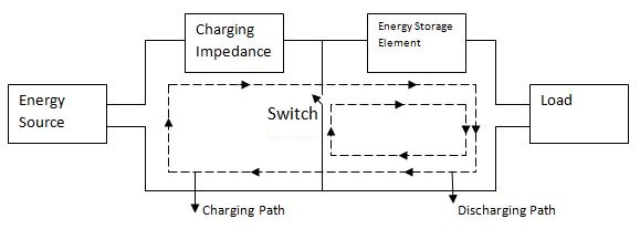 |
| Radar Modulator Block Diagram |
• Line Type Modulator:
In this device, a delay line or pulse forming network is used as storage element. The switch can be a Silicon Controlled Rectifier (SCR) that can initiate the discharge of pulse forming network to form a rectangular pulse. The shape and duration of the pulse are determined by passive elements of pulse forming network. This type of modulator is simple, compact in size and can tolerate abnormal load conditions.
• Active Switch Modulator: