
Noise Margin in Logic Families
 The margin in the noise voltage levels as explained above is called as the noise margin of the gate. Typical value of noise margin of TTL gates is 0.4 V. Thus from definition, we find:
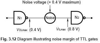
Figure 3.12 shows a TTL NAND gate N1 driving another TTL NAND gate N2. Assume that N1 is in the ON-state with VOLmax = 0.4 V and N2 is in the OFF-state with VILmax = 0.8 V. We find that in between N1 and N2, a maximum noise voltage of +0.4 V may be introduced without producing a triggering of N2. This means that the gates working in a noisy atmosphere can tolerate noise voltages of up to + 0.4 V. Similarly, if N1 is OFF with the output voltage VOH = 2.4 V, and N2 is ON with VIH = 2.0 V, the noise margin will be 2.4 − 2.0 = 0.4 V. In this case, the noise voltage is negative, as we have to subtract it from the input.
+Vnm = VILmax – VOLmax
‒Vnm = VOHmax – VIHmax
In the case of CMOS, the noise, we find that noise margin is quite high, and hence they highly suitable for working in industrial atmospheres. For CMOS gates, VIH = 7 to 10 volts. VIL = 0 to 3 volts, VOH = VDD, and VOL = 0 to 0.05 volt. Hence, Vnm( CMOS) = VDD.
Noise Immunity in Logic Families
Noise immunity of a TTL gate represents its ability to withstand the interference of noise in its smooth operation. This is a term derived from the theory of noise voltages. Noise margins of TTL gates were found to be equal to ±0.4 volt. We then say that these gates are immune to noise up to ±0.4 V. Noise immunity of CMOS gates is equal to VDD.
Propagation Delay tP
Propagation delay is defined as the time taken by a signal to get transmitted through an IC gate. Typical value of tP lies in the range of a few nanoseconds.