
We know that the basic building blocks of all electronic circuits are devices having controlled flow of electrons. Such devices are mostly vacuum tubes (or valves) before the discovery of transistors in 1948. Vacuum tubes includes vacuum diode with two electrodes, an anode and a cathode; triode with three electrodes - i.e., cathode, plate(anode) and a grid; tetrode - with four electrodes and pentode with five electrodes. In a vacuum tube, the inter-electrode space requires vacuum, it is to avoid lose of energy due to collision with air molecules. The heated cathode in the vacuum tube supplies the electrons and the varying voltage between the electrodes provides the flow of electrons in a controlled manner. Here the electrons flows in one direction, ice, from cathode to anode; hence they are called as valves. But vacuum tubes have many disadvantages: vacuum tubes are bulky, and requires high voltage for it to operate (~100 V), high power consumption and also it has limited life and the reliability is low. The number and the direction of flow of charge carriers are controlled by some semiconductors and their junctions. The number of mobile charges in a semiconductor can be changed by application of light, heat or small applied voltage. In the semiconductor device, the supply and flow of charge carriers are within the solid state and large evacuated space or external heating is not required. They have many advantages over the vacuum tubes like smaller size, consumption of low power, low power of operation and has high reliability and long life. In computer monitors and television, the CRT (Cathode Ray Tube) was used earlier, which works on the principle of vacuum tubes, now it is being replaced by LCD (Liquid Crystal Display) with supporting solid state electronics.
Classification of Metals, Conductors and Semiconductors on the basis of conductivity:
Based on the relative values of electrical conductivity (σ) or resistivity (ρ=1/σ), the solids are broadly classified as:


Even though the above description is grossly approximate and hypothetical, it helps to understand the difference between metals, insulators and semiconductors (extrinsic and intrinsic) in a simple way. The difference in the resistivity of C, Si and Ge mainly depends upon the energy gap between their valence and conduction bands. The energy gaps for C (diamond), Si and Ge, are 5.4 eV, 1.1 eV and 0.7 eV respectively. We know that Sn is also an element of group IV, but it is a metal because the energy gap in its case is 0 eV. Figure 6 shows the energy bands of n-type and p-type semiconductors.
Classification of Metals, Conductors and Semiconductors on the basis of conductivity:
Based on the relative values of electrical conductivity (σ) or resistivity (ρ=1/σ), the solids are broadly classified as:
(i) Metals: Metals possess very low resistivity or high conductivity.
р ~ 10-2-10-8 Ω m
(ii) Semiconductors: Semiconductors have resistivity or conductivity intermediate to metals and insulators.
р ~ 10-5-10-8 Ω m
σ ~ 105-10-6 S m-1
(iii) Insulators: Insulators possess high resistivity or low conductivity.
р ~ 1011-1019 Ω m
σ ~ 10-11-10-19 S m-1
The values of р and σ given above are indicative of magnitude and may go outside the ranges as well. Relative values of the resistivity are not the only criteria for the distinguishing of metals, semiconductors and insulators from each other. Most of the currently available semiconductor devices are based on elemental semiconductors Si or Ge and compound inorganic semiconductors. After 1990, a few semiconductor devices using organic semiconductors and semiconducting polymers have been developed signaling the birth of a futuristic technology of polymer-electronics and molecular-electronics.
On the Basis of Energy Bands:
Based on Bohr atomic model, "In an isolated atom, the energy of any of its electrons is decided by the orbit in which it revolves". But when solids are formed, the atoms come together in such a way that outer orbits of electrons would become very close or even overlap. Hence the motion of electrons in a solid is very different from that in an isolated atom. Each electron inside the crystal has got a unique position and no two electrons are having exactly same pattern of surrounding charges.
Each electron inside the crystal has got a unique position and no two electrons are having exactly same pattern of surrounding charges. These different energy levels with continuous energy variation form can be called as energy bands. The energy level of valence electrons is included in the energy band called as valence band. The energy band above the valence band can be called as the conduction band. All the valence electrons will reside in the valence band due to the absence of external energy. The electrons from the valence band can easily move into the conduction band, if the lowest level in the conduction band happens to be lower than the highest level of the valence band. Usually the conduction band is empty. But, electrons from the valence band moves freely into the conduction band when both the bands overlaps. This occurs in case of metallic conductors.
Electrons in the valence band all remain bound and no free electrons are available in the conduction band, when there is some gap between the conduction band and the valence band. This makes a material as an insulator. Some of the electrons in the valence band may gain external energy and cross the gap between the conduction band and the valence band. Then these types’ electrons will move to the conduction band. These electrons will create vacant energy levels in the valence band, where other valence electrons can move. Thus this process makes the possibility of conduction due to the electrons present in the conduction band and the vacancies present in the valence band.
Now consider the case of Si or Ge crystal containing N atoms. We know that for Si, the outermost orbit is third orbit (n=3) and for Ge, it is the fourth orbit (n=4). The number of electrons present in the outermost orbit is 4 (2s and 2p electrons). Thus, the total number of electrons present in the outer orbit of the crystal is 4N. The maximum number of electrons present in the outer orbit is 8 (2s + 6p electrons). So, for the 4N valence electrons, there exist 8N available energy states. Depending up on the distance between the atoms in the crystal, these 8N discrete energy levels can either form a continuous band or they may be grouped in different bands.
The energy band of these 8N states is split apart into two which are separated by an energy gap Eg. The valence band is the lower band, which is completely occupied by the 4N valence electrons at temperature of absolute zero. The other band consisting of 4N energy states and is completely empty at absolute zero is called the conduction band.
Band Theory of Solids :
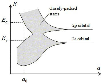
Consider that N atoms are present in the Si or Ge crystal. In different orbits, electrons of each atom will have discrete energies. If all atoms are isolated, the electron energy will be same i.e. separated from each other by a large distance. The atoms are close to each other (2 to 3 Å) in a crystal and therefore the electrons interact with each other and also with the neighboring atomic cores. In the outermost orbit, the interaction (overlap) will be more felt by the electrons, while the inner orbit or the core electron energies may remain unaffected. So we need to consider the changes in the energies of the electrons present in the outermost orbit only for understanding the electron energies in Si or Ge crystal. The outermost orbit for Si is the third orbit (n=3) and for Ge, it is the fourth orbit (n=4). The total number of electrons present in the outermost orbit is 4 (2s and 2p electrons). Hence the total number of outer electrons present in the crystal is 4N. The maximum possible number of outer electrons present in the orbit is 8 (2s+6p electrons). So, out of the 4N electrons, 2N electrons are in the 2N s-states (orbital quantum number l =0) and the 2N electrons are present in the available 6N p-states. This is the case of well separated or isolated atoms.
If these atoms start coming nearer to each other to form a solid, the energies of these electrons in the outermost orbit may change (both increase and decrease) due to the interaction between the electrons of different atoms. The 6N states for l=1, originally having identical energies in the isolated atoms, spread out to form an energy band. Similarly, the 2N states for l=0, having identical energies in the isolated atoms, split into a second band, separated from the first one by an energy gap. Figure 1.1shows The Band Theory of Solids.

Figure 1.1: Band Theory of Solids
At smaller spacing, there comes a region in which the bands merge with each other. The lowest energy state that is a split from the upper atomic level appears to drop beneath the upper state that comes from the lower atomic level. No energy gap exists in this region, where the lower and upper energy states get mixed. Figure 1.2 shows the conductivity of Conductors, semiconductors and insulators with the increase of temperature.

Figure 1.2 : Conductivity of Conductors, semiconductors and insulators with the increase of temperature.
The energy bands again split apart and are separated by an energy gap Eg when the distance between the atoms decreases. The total number of available energy states 8N has been re-apportioned between the lower and upper energy bands each of 4N states. Here there are exactly many states in the lower band (4N) as there are available valence electrons from the atoms (4N). So this band, the valence band is completely filled while the upper band, the conduction band is completely empty.

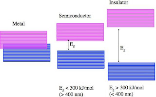
Figure 2 : Difference between energy bands of metals, insulators and semiconductors.
The Energy band gap is the gap between the top of the valence band and the bottom of the conduction band. Depending upon the material, it may be large, small or zero. We can classify materials into conductors, insulators and semiconductors based on the energy gap. Figure 2 shows the difference between energy bands of metals, insulators and semiconductors.
Conductors:
In case of conductors, the valence band and the conduction band overlaps. Here there is overlap electrons from valence band can easily move into the conduction band. This makes a large number of electrons available for electrical conduction. If the valence band is partially empty, the electrons from its lower level can move into the higher level. This makes conduction possible. So the resistance of such materials is low or the conductivity is high.
Insulators:
In this case, a large energy band gap Eg (Eg >3 eV) exists between the two bands. Here no electrical conduction is possible, due to the absence of electrons in the conduction band. In case of insulators, the energy gap is very large that electrons cannot be excited from the valence band to the conduction band by thermal excitation.
Semiconductors:
Here in this case, a finite but small band gap (Eg <3 eV) exists. At room temperature, some electrons from valence band can acquire enough energy to cross the energy gap and enter the conduction band due to the small band gap. These electrons (in small numbers) can move in the conduction band. Thus the resistance of semiconductors is not high as that of insulators. Now we are discussing about the types of semiconductors
1. Intrinsic Semiconductors:
The lattice structures of Si and Ge are commonly called as the diamond-like structures. In this type of structure, each atom is surrounded by four nearest neighbors. We know that the valence electrons of Si and Ge atoms are four. Every Si or Ge tends to share one of its four valence electrons with each of its four nearest neighbor atoms, and also to take share one electron from each such neighbor in its crystalline structure. These shared electron pairs are capable to form a covalent bond or also referred to as valence bond. These two shared electrons are to shuttle back-and-forth between the associated atoms holding together them strongly.

Figure 3.1: Three dimensional diamond-like crystal structure for C,Si or Ge.

Figures 3.2 shows an idealized picture in which no bonds are broken or all bonds are intact. At low temperature condition only these situation arises. By the gradual increase of temperature, more thermal energy becomes available to these electrons and some of these electrons can break-away, i.e. becoming free electrons contributing to conduction. In the bond, the thermal energy effectively ionizes only a few atoms in the crystalline lattice and creates a vacancy. The atoms from which the free electrons, with charge (–q) is released by leaving a vacancy has got an effective charge of (+q). This effective positive electronic charge constituting a vacancy is referred to as a hole. The hole can be considered as an apparent free particle with effective positive charge.
In an intrinsic semiconductor, the number of free electrons (ne) equals the number of holes (nh). That is:
ne = nh = ni,
Where, ni is called as the intrinsic carrier concentration.
Figure 4.1 shows the schematic two-dimensional representation of si or Ge structure showing covalent bonds at low temperatures.

Figure 4.1 : Schematic two-dimensional representation of si or Ge structure showing covalent bonds at low temperatures
The semiconductor materials posses an unique property, that is apart from the electrons, the holes can also move. Figure 4.1 shows the schematic two-dimensional representation of si or Ge structure showing covalent bonds at low temperatures.
Let us consider that there is a hole in figure 4.2. An electron from the covalent bond may jump to the vacant site (hole). Thus after a jump, the hole is at the new site and an electron is present in the old site . Thus we can say that apparently, the hole has moved from one site to other site. The free electrons moves completely independently as conduction electron and gives rise to an electron current, Ie under an applied electric field and is not involved in the process of hole motion. It should be remembered that the motion of hole is only a convenient way of describing the actual motion of bounded electrons, whenever there exists an empty bond anywhere in the crystal. These holes move towards negative potential and giving the hole current Ih under the action of an electric field. Thus the total current I is the sum of the electron current Ie and the hole current Ih.
I = Ie + Ih
Apart from the process of generation of conduction electrons and holes, a simultaneous process of recombination occurs, in which the electrons recombines with holes. The rate of generation is equal to the rate of recombination of charge carriers at equilibrium state. When an electron collides with a hole, the recombination process occurs. Figure 4.2 shows the schematic model of generation of hole due to thermal energy at moderate temperatures

Figure 4.2: schematic model of generation of hole due to thermal energy at moderate temperatures
When T=0K, an intrinsic semiconductor behaves like an insulator. At higher temperatures (T>0K), due to the thermal energy, some electrons excites from the valence band to the conduction band. These thermally excited electrons (T>0K), partially occupies in the conduction band. Hence in the energy band diagram of an intrinsic semiconductor, some electrons can be shown in the conduction band. These electrons have come from the valence band by leaving equal number of holes there. Figure 4.3 shows an Intrinsic semiconductor at T=0 K behaves like insulator and at T>0 K, four thermally generated electron hole pair. Figure 4.3 shows an Intrinsic semiconductor at T=0 K behaves like insulator and at T>0 K, four thermally generated electron hole pair.

Figure 4.3 : An Intrinsic semiconductor at T=0 K behaves like insulator and at T>0 K, four thermally generated electron hole pair
Here there may arise a question that why Carbon (C) is an insulator while Si and Ge are intrinsic semiconductor although Si, Ge and C have same lattice structures?
We know that the four bonding atoms of C, Si or Ge lies respectively in the second, third and fourth orbit. Hence the ionization energy (Eg), the energy required to take out an electron from these atoms will be least for Ge, followed by silicon and highest for C. Hence the number of free electrons for conduction in Si and Ge are significant and in case of C, which is negligibly small.
2. Extrinsic Semiconductors:
We know that the conductivity of an intrinsic semiconductor mainly depends on its temperature, but at room temperature, its conductivity is very low. Thus it is not possible to develop important electronic devices by using these types of semiconductors. The conductivity of these materials can be improved by making the use of impurities.
The conductivity of the semiconductor is increased manifold when small amount, say, a few parts per million (ppm) of a suitable impurity is added to the pure semiconductor material. These types of materials are commonly known as extrinsic semiconductors or impurity semiconductors. Doping is the process of deliberate addition of a desirable impurity and the impurity atoms are called as dopants. Such material is also referred to as doped semiconductor. The dopant should be selected such that it does not distort the original pure semiconductor lattice. Of the original semiconductor atom sites in the crystal, only a very few portions occupies by the dopants. In order to attain this, it should satisfy a necessary condition that the sizes of the dopant and the semiconductor atoms should be nearly the same.
For the doping of the tetravalent Si or Ge atoms, two types of dopants are used:
1. Pentavalent dopants like Arsenic (As), Antimony (Sb), Phosphorous (P) etc having valency 5.
2. Trivalent dopants like Indium (In), Boron (B), Aluminium (Al) etc having valency 3.
Now we discusses the process of how the doping changes the number of charge carriers (and hence the conductivity) of semiconductors. Since Si or Ge belongs to the fourth group of the periodic table, we choose the dopant elements from the fifth or third group elements, which are near by the fourth group, expecting and taking care that the size of the dopant atom is nearly the same as that of Si or Ge. The Pentavalent and trivalent dopants in Si or Ge give two entirely different types of semiconductors.
(i) n- type semiconductor:
Here we dope Si or Ge with a pentavalent element. In the crystal lattice of Si when an atom of +5 valency element occupies the position of an atom, four of its electron bonds with the four silicon neighbours while the fifth remains very weakly bound to its parent atom. This is due to the four electrons participating in bonding are seen as part of the effective core of the atom by the fifth electron. Hence the ionization energy needed to set this electron free is very small. So even at room temperature, it will be free to move in the lattice of the semiconductor. For example, the energy required to separate this electron from its atom for germanium is ~ 0.01 eV and 0.05 eV for silicon. This is in contrast to the energy required to jump the forbidden band at room temperature in the intrinsic semiconductor is about 0.72 eV for germanium and about 1.1 eV for silicon. Hence the Pentavalent dopant is donating one extra electron for conduction and is referred to as donor impurity. The number of electrons available for conduction by dopant atoms strongly depends upon the doping level and is independent of any increase in the ambient temperature. Also the number of free electrons generated by Si atoms (with an equal number of holes) increases weakly with temperature.
The total number of conduction electrons ne in a doped semiconductor is mainly due to the electrons contributed by donors and those generated intrinsically. The total number of holes nh is only due to the holes from the intrinsic source. Due to the increase in the number of electrons, the rate of recombination of holes would also increases. Hence the number of holes would get further reduced. Figure 5.1 shows the Pentavalent donor atom P doped for tetravalent Si giving n-type semiconductor.

Figure 5.1 : Pentavalent donor atom P doped for tetravalent Si giving n-type semiconductor.
Thus the number of conduction electrons can be made much larger than the number of holes with the help of proper level of doping. Thus in an extrinsic semiconductor doped with the pentavalent impurity, electrons are the majority carriers and holes are the minority carriers. Hence these semiconductors are also known as n-type semiconductors. For n-type semiconductors, it is clear that ne>> nh.
(ii) p-type semiconductors:
The p-type semiconductor materials can be obtained when Si or Ge is doped with a trivalent impurity like Al, B, In, etc. Due to the trivalent impurity dopants, the dopant has one valence electron less than Si or Ge. Hence this atom can form covalent bonds with neighbouring three Si atoms and does not have any electron to offer to the fourth Si atom. So the bond between the fourth neighbour and the trivalent atom has a vacancy or also known as a hole. The neighbouring Si atom in the lattice needs an electron in place of a hole; an electron in the outer orbit of an atom in the neighbourhood may jump to fill this vacancy, by leaving a vacancy or hole at its own site. Thus in p-type semiconductor, hole is available for conduction. When the trivalent foreign atom shares fourth electron with the neighbouring Si atom, it becomes effectively negatively charged. Thus the dopant atom of p-type material can be considered as core of one negative charge along with its associated hole. It is very clear that one acceptor atom gives one hole. These holes are in addition to the intrinsically generated holes. The source of conduction electrons is only intrinsic generation. Hence for these types of materials, holes are the majority carriers and electrons are minority carriers. Hence extrinsic semiconductors doped with trivalent impurity are called p-type semiconductors. The recombination process will reduce the number (ni) of intrinsically generated electrons to ne for p-type semiconductors. Thus for p-type semiconductors, nh>>ne.
The crystal maintains an overall charge neutrality as the charge of additional charge carriers is just equal and opposite to that of the ionized cores in the lattice. Because of the abundance of majority current carriers in the extrinsic semiconductors, the minority carriers produced thermally have more chance of meeting majority carriers and thus getting destroyed. Hence the dopants become the majority carriers by adding a large number of current carriers of one type indirectly help to reduce the intrinsic concentration of minority carriers. Figure 5.2 shows the trivalent acceptor atom B doped in tetravalent Si lattice giving p-type semiconductor.

Figure 5.2 : Trivalent acceptor atom B doped in tetravalent Si lattice giving p-type semiconductor.
The energy band structure of the semiconductor is affected by doping. The additional energy states due to donor impurities (ED) and acceptor impurities (EA) also exist in case of extrinsic semiconductors. The donor energy level (ED) is slightly below the bottom EC of the conduction band in the energy band diagram of n-type Si semiconductor and electrons from this level move into the conduction band with very small supply of energy. Most of the donor atoms get ionized at room temperature, but very few (~10-12) atoms of Si get ionized. Thus the conduction band has most electrons coming from the donor impurities. In the similar way, for p-type semiconductor, the acceptor energy level (EA) is slightly above the top of EV of the valence band. An electron from the valence band can jump to the level EA and ionize the acceptor negatively, with very small supply of energy. In other words, we can also say that with very small supply of energy the hole from level EA sinks down into the valence band. When they gain external energy, electrons rise up and holes fall down. Most of the acceptor atoms get ionized leaving holes in the valence band at room temperature. Thus the density of holes in the valence band is predominantly due to impurity in the extrinsic semiconductor at room temperature. In thermal equilibrium, the electron and hole concentration in a semiconductor is given by,

Even though the above description is grossly approximate and hypothetical, it helps to understand the difference between metals, insulators and semiconductors (extrinsic and intrinsic) in a simple way. The difference in the resistivity of C, Si and Ge mainly depends upon the energy gap between their valence and conduction bands. The energy gaps for C (diamond), Si and Ge, are 5.4 eV, 1.1 eV and 0.7 eV respectively. We know that Sn is also an element of group IV, but it is a metal because the energy gap in its case is 0 eV. Figure 6 shows the energy bands of n-type and p-type semiconductors.
Tags:
Semiconductors
good
ReplyDelete