
The NMOS NAND Gate Circuit
Figure 3.22(a) shows a two-input NMOS NAND gate circuit. This circuit is a modification of the NAND gate using mechanical switches shown in Fig. 3.22(b). The mechanical switches of Fig. 3.22(b) are replaced with NMOS transistors in Fig. 3.22(a). NMOS transistors T2 and T3 are of the enhancement type and T1, which acts as the load resistance, is of the depletion type. Note that this load is located on top of the switching transistors T2 and T3 to produce inversion. If A = 0 and B = 0 (i.e., A and B have 0-volt inputs), transistors T2 and T3 will remain OFF. Then, the output Z = +VDD (logic 1). The same situation prevails, when A = 0 and B = 1, or B = 0 and A = 1. Now, if A = B = 1, then both T2 and T3 will conduct and the output Z = 0. These logic operations are summarized as given in Table 3.3, which suggests that the gate shown in Fig. 3.22(a) is a positive-logic NAND gate. To get a negative-logic NAND gate, we replace the NMOS transistors with PMOS transistors.
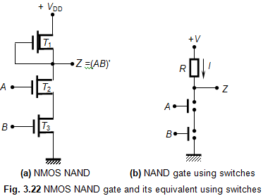
Figure 3.22(a) shows a two-input NMOS NAND gate circuit. This circuit is a modification of the NAND gate using mechanical switches shown in Fig. 3.22(b). The mechanical switches of Fig. 3.22(b) are replaced with NMOS transistors in Fig. 3.22(a). NMOS transistors T2 and T3 are of the enhancement type and T1, which acts as the load resistance, is of the depletion type. Note that this load is located on top of the switching transistors T2 and T3 to produce inversion. If A = 0 and B = 0 (i.e., A and B have 0-volt inputs), transistors T2 and T3 will remain OFF. Then, the output Z = +VDD (logic 1). The same situation prevails, when A = 0 and B = 1, or B = 0 and A = 1. Now, if A = B = 1, then both T2 and T3 will conduct and the output Z = 0. These logic operations are summarized as given in Table 3.3, which suggests that the gate shown in Fig. 3.22(a) is a positive-logic NAND gate. To get a negative-logic NAND gate, we replace the NMOS transistors with PMOS transistors.
Table 3.3 NMOS NAND
A | B | Z |
0 0 1 1 | 0 1 0 1 | 1 1 1 0 |