
The NMOS AND Gate Circuit
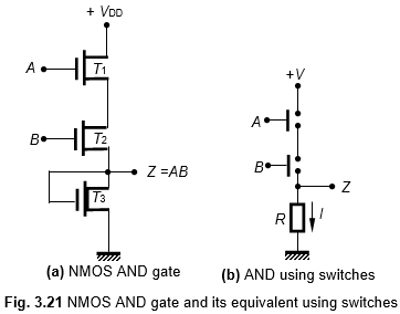
Figure 3.21(a) shows a two-input AND gate using NMOS field-effect transistors. This diagram is a modification of the AND gate using switches shown in Fig. 3.21(b). The AND gate constructed using mechanical switches was discussed in Section 24 using Fig. 2.4. Figure 3.21(b) is a reproduction of Fig. 2.4 for reference. The mechanical switches of 3.21(b) are replaced with NMOS transistors in Fig. 3.21(a). We find that in Fig. 3.21(a), if A = 0 and B = 0 (i.e., A and B have 0-volt inputs), transistors T1 and T2 will remain in the OFF-state. Then, output Z = 0 volt (logic 0). The same situation prevails, when A = 0 and B = 1, or B = 0 and A = 1 (here logic 0 = 0 volt). Now, if A = B = 1, then both T1 and T2 conduct and develop +VDD, across the load transistor T3. This means that the output Z = logic 1. These may be summarized as given Table 3.2. The entries given in Table 3.2 are found to be that of the AND operation. So, we conclude that the logic gate shown in Fig. 3.21(a)- performs the positive-logic AND operation.
Table 3.2 NMOS AND
A | B | Z |
0 0 1 1 | 0 1 0 1 | 0 0 0 1 |
Nice! Thanks for this and other posts.
ReplyDelete