
(a) Logic Analyzer:
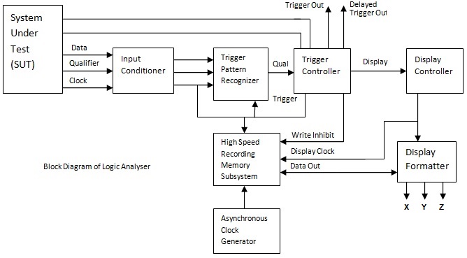
The most popular test instrument for trouble shooting digital and microprocessor based systems is the logic analyser. Its appearance is similar to CRO but it looks into the activity on the communicating links in a digital system known as interface buses. Since an interface bus is a parallel assembly of connections, data is transmitted as parallel bit streams. Thus, at discrete instants in time data words are formed and this form of activity takes place in the data domain. Figure shows the simplified block diagram of a logic analyser. This diagram does not include the display system which is normally on a CRT.
 |
| Logic Analyzer Block Diagram |
• Data, qualifier and clock signals from the System Under Test (SUT) are received at the input-conditioner block. This block ensures that the loading on the SUT because of the logic analyser is minimal, compensates for the deterioration in signal characteristics due to capacitance loading (the capacitance is capable of carrying the high speed signals for the SUT to the logic analyser) and ensures a minimum data/ qualifier set up time and a zero data/qualifier hold time.
• It also carries out the function of threshold detection and level conversion since signals from the SUT may conform to one of many different logic families used in modern electronic equipment.
• The conditioned data and qualifier signals next go to the Trigger Pattern Recogniser (TPR) block.
• This block provides for the setting of a combinational trigger word and produces an output called Qualified Trigger (QT) when the trigger word pattern set matches an input data plus qualifier pattern.
• The data signals simultaneously go to the High Speed Acquisition Memory Subsystem where they are stored at the SUT clock rate or at a rate governed by the internal asynchronous clock generator.
• The memory subsystem continuously writes (stores) input data till such time that the trigger controller inhabits the writing process.
• Since the logic analysers contain finite memory, say "m” words, the memory subsystem will always contain the "m” most recent word of input data.
• The trigger controller block on receipt of the qualified trigger signal from the trigger pattern recogniser ensures that requisite trigger conditions are satisfied before signaling the memory subsystem to stop writing and instructing the Display controller to take over by reading data at a rate governed by the display clock.
• The data read out is taken up by the display for matter for appropriate representation on the CRT screen.
• In order to examine the activity, multiline data process is required. In the modern logic analysers, the options available for setting up the equipment are displayed as a menu on the screen with a cursor to indicate the next input required.
• The keyboard is used to enter the information to give the required operating sequence.
• The logic analysers are usually provided with a series of Personality Modules to reconfigure the equipment for a wide range of microprocessors.
• These units may be as simple as four input AND gates for connection to the oscilloscope trigger input and would synchronize the oscilloscope with the occurrence of a particular parallel work.
(b) Applications of Logic Analyzers:
Logic Analyzers are useful:
1. For hardware and software engineers in their R & D work.
2. For Testing, debugging and designing in microprocessors application field.