
In TTL circuits also, input transistor T1 is a multi-emitter transistor driving the phase-splitter transistor T2. As stated above, this phase-splitter drives the push-pull output transistors T3 and T4. The output section, consisting of transistors T3 and T4, diode D, and the 100-ohm resistor, is known as a totem-pole configuration, since it looks like a totem-pole with its ups and downs. It may be noted that a totem pole is a stick held by kings, emperors, and holy men in their hands to exhibit their authority. In another type of NAND gate, called the open-collector NAND gate, transistor T3 and diode D are removed.
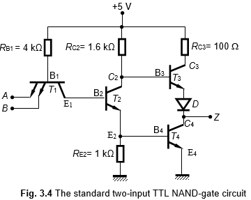
Now consider the condition A = B = 1. In this case, both the diodes A and B remain reverse biased. So, current flows from +VCC through the base-collector diode of T1 into the base of T2 turning it ON. Collector current of T2 starts flowing now, developing enough voltage (0.8 V) at its emitter E2 to turn T4 ON. Also since T2 is ON, its collector-emitter voltage drops to the saturation value of VCES2 = 0.2 V and its collector voltage VC2 = 0.8 + 0.2 = 1 V. With diode D present, T3 remains OFF. However since T4 is ON, the collector-emitter voltage of T4, VCES4 = 0.2 V, and the output Z is at logic 0. Thus for the situation A = B = 1, we have Z = 0. These relations are summed up as shown in Table 3.1. Inspection of the entries in Table 3.1 reveal that the circuit shown in Fig. 3.4 acts as a two-input positive-logic NAND gate.
Consider the situation when both the inputs A and B are at the logic-0 (0-V input) state, i.e., A = B = 0. In this condition, the base-emitter diodes of the multi-emitter transistor T1 are forward biased and current flows from +VCC through the base and emitters of T1 to ground. This makes the base-collector diode of T1 reverse biased, and prevents current from flowing into the base of transistor T2. Since there is no current flow through its base, T2 remains OFF making its collector current IC2 = 0, and collector voltage VC2 = +VCC (+5 V as standard value for TTL family). We also find that since the collector current of T2 is zero, its emitter voltage VY = 0.
Let us now investigate the states of the totem-pole transistors T3 and T4. Since the collector voltage of T2, VC2 = VCC, transistor T3 turns-on and it acts as a short circuit between VCC and output point Z. Also since the emitter voltage of T2, VE2 = 0, transistor T4 remains OFF. Since T3 is ON and T4 is OFF, we find that the output Z for the input condition A = B = 0, is +VCC, or logic 1.
Consider now the situations in which A = 1 and B = 0, or A = 0 and B = 1. In these cases also, one of the diodes is conducting and the input is grounded. So the same arguments given above for the situation A = B = 0 prevails in these cases also.
Now consider the condition A = B = 1. In this case, both the diodes A and B remain reverse biased. So, current flows from +VCC through the base-collector diode of T1 into the base of T2 turning it ON. Collector current of T2 starts flowing now, developing enough voltage (0.8 V) at its emitter E2 to turn T4 ON. Also since T2 is ON, its collector-emitter voltage drops to the saturation value of VCES2 = 0.2 V and its collector voltage VC2 = 0.8 + 0.2 = 1 V. With diode D present, T3 remains OFF. However since T4 is ON, the collector-emitter voltage of T4, VCES4 = 0.2 V, and the output Z is at logic 0. Thus for the situation A = B = 1, we have Z = 0. These relations are summed up as shown in Table 3.1. Inspection of the entries in Table 3.1 reveal that the circuit shown in Fig. 3.4 acts as a two-input positive-logic NAND gate.
Truth table of two-input TTL NAND
A | B | Z |
0 | 0 | 1 |
0 | 1 | 1 |
1 | 0 | 1 |
1 | 1 | 0 |
Great explanation, certainly better than my textbook
ReplyDeleteGreat Explanation! However, the output of the truth table appears to be a NOR gate.
ReplyDeleteNo it's right the output is for NAND gate
DeleteWhen T3 is ON, how do you determine whether it is in Saturation or Active mode? And if T3 is in Saturation, do you need to put a load at Z to find Vout? I ask this because if T3 is in Saturation you can not use the Ic=B*Ib relationship.
ReplyDelete