
Viva Questions and Answers on Bipolar Junction Transistor Experiment
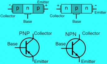
In a Bipolar Junction Transistor, the current flow is mainly due to two polarities, holes and electrons. A BJT has three terminals, namely emitter, base and collector. BJT can be of two types, PNP or NPN transistor. Out of these two, NPN transistor is the best one and is most commonly used one. For NPN transistor, the mobility of electrons is more than that of holes. Due to this reason, the electron current is more than the hole current in NPN transistor.


1. Briefly discuss about a transistor?
We can simply say that, a “junction transistor is simply a sandwich of one type of semiconductor material between two layers of the other type”. A transistor has three terminals namely emitter, base and collector. A transistor is a current sensing device. Transistor was developed in the year 1948 at BELL laboratories. A transistor can be seen as two p-n junction placed back to back. The emitter is heavily doped, while the base is lightly doped. The collector is moderately doped. A transistor can be considered as the heart of electronic products. It is almost used in all electronic devices. There are mainly two types of transistors namely, pnp and npn transistors.
2. Discuss about a Bipolar Junction Transistor (BJT), explain about its terminals, types, and mention which type is better? Justify your answer?
In a Bipolar Junction Transistor, the current flow is mainly due to two polarities, holes and electrons. A BJT has three terminals, namely emitter, base and collector. BJT can be of two types, PNP or NPN transistor. Out of these two, NPN transistor is the best one and is most commonly used one. For NPN transistor, the mobility of electrons is more than that of holes. Due to this reason, the electron current is more than the hole current in NPN transistor.
3. Mention about the different configurations of a transistor?
The different configurations of a transistor are common emitter configuration, common base and common collector configurations.
a) Common Emitter (CE)

b) Common Base (CB)
c) Common collector(CC)
4. Explain about the Common Base configuration?
In a common base configuration, the base terminal is common between the input and output circuits. The applied input signal is fed to the emitter-base terminal and the output is collected from the collector-base terminal.
5. Discuss about the characteristics of CB configuration?
We know that, the input resistance of a CB configuration is low and the output resistance is high. Due to this, the current gain of a CB configuration is less than 1. The input and output signals in the common-base circuit are always in phase. The configuration of a CB is mentioned in question 4.
6. Mention about a transistor and explain why it is called so?
The explanation of transistor is mentioned in question number 1. The transistor got its name because a transistor transfers the input signal from low resistance to high resistance. There are mainly two types of transistors-pnp and npn.
7. Explain the parameters α, β, γ in transistor. Give the relation between them?
These parameters represent current gains in CB, CE and CC configurations respectively.
8. Give the comparison of common emitter, common base and common collector configurations?
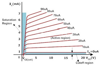
9. Define cut-off, active and saturation regions in a transistor?
The operation of a transistor can be defined in three regions namely active region, saturation region and cut-off region.
Cut off region: In a cut-off region, both the emitter junction (Je) and the collector junction (Jc) are in reverse biased condition
Active region: In an active region, the emitter junction is forward biased condition and the collector junction is reverse biased.
Saturation region: In a saturation region, both the emitter and collector junctions are in forward biased condition.
10. How you understand about input and output characteristics?
We can say that the Input Characteristics describes the changes in input current with the variation in the values of input voltage keeping the output voltage constant. The output characteristics can be defined as the plot of output current versus output voltage with constant input current.
11. How you explain about the physical structure of a BJT?
A typical BJT can be seen as one N type material is sandwiched between two P type materials or One P type material is sandwiched between two N type materials, The physical structure of a BJT has its widths (Collector>Emitter>Base) and the ratio of doping concentration (Emitter>Collector>Base).
12. Discuss in detail about Early Effect?
The Early effect can be defined as; it is the variation in base width of BJT due to variation in the applied base-collector voltage.
13. How you understand about the emitter current increase with increase in reverse bias at the collector junction?
It is due to the effect of breakdown at collector junction.
14. What you understand about the collector reverse saturation current?
The reverse saturation current is the current due to the minority carriers flow through collector junction when it is connected in reverse bias.
15. Give the collector current expression for BJT in Common Base configuration?
At the Cut-off region, Ic= 0
Active region Ic= βIb
Saturation Ic < βIb
16. What is the value of VCE Sat for the transistor BC107?
For BC107, Vce sat=0.2V
17. How a transistor performs as an electronic switch?
It is a well known fact that transistor is commonly used as switch in electronic circuits. We know that, when transistor is in cut off region, it works as off switch (off state condition) and when transistor is in saturation region, it works as on switch (on state condition).
18. Explain whether a BJT is a current controlled device or a voltage-controlled device?
BJT is a current controlled current device
19. Give the representations of NPN and PNP transistors.
20. Give the characteristics of a common emitter BJT configuration.
21. How a common-emitter configuration gets its name?
In a common emitter configuration, the emitter terminal is common to both input and output. That is for both the input and output, the base region is needed.
22. Define “load-line”. And give its significance? Compare a.c. load line and d.c. load line.
The load line specifies the operating point (Q point) of a transistor. Dc load line can be defined as the line based on the relation between output voltage and currents when input is zero, Ac load line is the line which process through the Q point with slope of (-1/Rac, Rac= Rc//Rl).
23. What you understand about Q- point?
The Q-point of a transistor specifies the correct biasing for the required amplification.
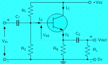
24. Explain about biasing and its need for transistors?
Biasing can be defined as the process of giving proper supply voltage and resistances for obtaining the desired operating point.For the proper working of transistor, biasing is needed. Without proper biasing, a transistor cannot work properly.
25. Explain about the different methods of transistor biasing. Which type is best and why?
The different types of transistor biasing are; Fixed bias, Emitter feedback bias, Collector to base bias, Collector- emitter feedback bias and self bias (voltage divider bias). Out of all these biasing techniques, voltage divider bias (self bias) is best and is commonly used, because self bias is more stable for a greater range of input signal
26. Define thermal runaway?
Thermal runaway is a situation where increase in temperature alters the conditions in a way that causes an additional increase in temperature.
27. What is the normal value of thermistor temperature co efficient?
The value of a thermistor temperature may be positive (+) or negative (–) based on the type of material used.
28. What is a two port network? Explain its types, and which one is best for BJT?
A two port network has two ports, input and output ports. Z, Y, h, g are the ABCD parameters of a two port network. The best one is hybrid parameters because this parameter gives all parameters about amplifier such as input, output impedance, voltage and current gains.
29. Give the h-parameter values for a transistor?
30. Give the comparison and applications of a CE, CB and CC amplifiers?
Property | CB | CE | CC |
I/P resistance | Low | Moderate | High |
O/P resistance | High | Moderate | Low |
Current Gain | 1 | High | High |
Voltage Gain | ≈150 | ≈ 500 | >1 |
Phase Shift | 0 or 360° | 180° | 0 or 360° |
Uses | High freq ckts | Audio freq ckts | For Impedance Matching |
Tags:
Viva Questions