
The Internal Block Diagram of 8086 Microprocessor is shown below.
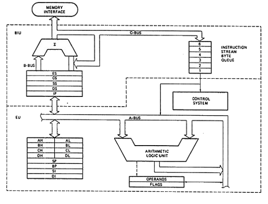
The functional block diagram of 8086 is divided into two functional units.
(1) Bus Interface Unit and (2) Execution Unit
They are explained below.
(1) Bus Interface Unit:
Bus Interface Unit is a gate (enhance) interface between peripheral devices and Processor. Through the bus interface only, processor can send and receive data. The bus interface unit contains
(a) Instruction Queue
(b) Segment Registers
(c) Instruction Pointers
(a) Instruction Queue
In 8086 Processor, instruction queue is a 6 byte register used to store permanent data from the Input/Output (I/O) devices or processor. The queue operates in the principle of First In First Out (FIFO) principle. i.e., the first data is fetched and that data will be taken out firstly.
(b) Segment Register:
In 8086 Processor, there are four segment registers. They are
ES – Extra Segment
CS – Code Segment
DS – Data Segment
SS – Stack Segment
The maximum memory access of 8086 processor is 1 MB. Each segment has some predefined functions.
In 8086 processor, each segment has a capacity of 64 KB. So the four segments will store 256 KB of memory locations. The remaining memory locations are free and in these locations, user can perform any other processes. These four segment registers will keep the base address of the corresponding segment.
(c) Instruction Pointer (IP):
Instruction pointer will give the next address of the instruction to be executed. Instruction Point cannot be used for other purposes.
(2) Execution Unit:
The execution unit contains
(a) Control Unit
(b) Instruction Decoders
(c) ALU
(d) General Purpose Registers
(e) Flag Registers
Address Generation:
The I/O processor can receive data from the memory only, if that data should goes out through the address generation.
General Purpose Registers:
AX, BX, CX, DX, SP, BP, SI, DI are General Purpose Registers.
1. AX register (Accumulator):
AX register can save 16 bit data only.
2. BX register:
BX register is the base register. It is used to save the base data (value).
3. CX register:
CX register is code register (Count Register)
4. DX Register:
DX register is data register. DX register is used to store datas.
5. SP (Stack Pointer):
Stack Pointer keeps the top of the stack. The stack pointer operates in the principle of Last In First Out (LIFO). Since one location can store only 8 bit data, in order to store a 16 bit data, two memory locations are needed. So the stack pointer will decreased by two memory locations, if a data is taken.
6. BP (Base Pointer):
Base pointer is used to store the base address of the memory or stack.
7. SI (Source Index):
Source Index is used to hold the index value of source operand for string instructions.
8. DI (Destination Index):
DI is used to hold the index value of destination operand for string instructions.
General purpose registers are used for holding data, intermediate results, counters, mode of addressing and also for storing effective address.
Flag Registers:
The three control flags are,
1. Trap Flag (TF)
2. Interrupt flag (IF)
3. Direction Flag (DF)
Instruction Format,
Instruction Format,
15 14 13 12 11 10 9 8 7 6 5 4 3 2 1 0
U | U | U | U | CF | DF | IF | TF | SF | ZF | U | AF | U | PF | V | CF |
Symbolic Representation,

Tags:
Microprocessors