
There are 40 pins in Intel 8085 microprocessor. The photo image is shown in figure and pin diagram is shown in figure.
The signals are classified into the following categories.
 |
| Intel 8085 microprocessor |
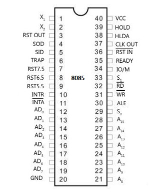 |
| Pin diagram of Intel 8085 microprocessor |
S.No. | Group |
1 | Address bus |
2 | Multiplexed Address / Data bus |
3 | Control and Status signals |
4 | Peripheral initiated signals |
5 | Clock signals |
6 | Reset signals |
7 | Interrupt signals |
8 | Serial I/O signals |
9 | Power supply and Ground signals |
The signal diagram is shown in figure below.
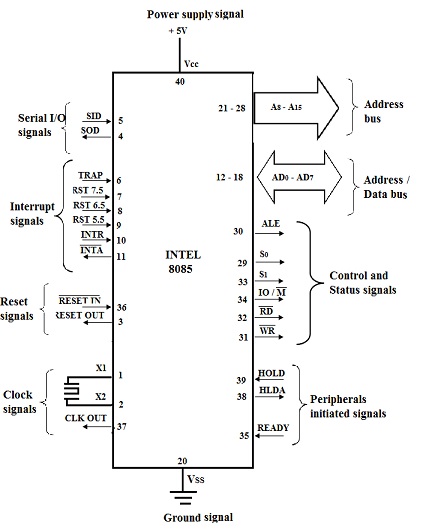 |
| Signal diagram of Intel 8085 microprocessor |
Pin number | Signal name | Description |
Address Bus | ||
21 – 28 | A8 – A15 | Higher order byte (8 bits) of address bus. The address bus is unidirectional (one-way, ie. microprocessor to memory). |
Multiplexed Address / Data bus | ||
12 -19 | AD0 – AD7 | Lower order byte (8 bits) address bus (A0 - A7). And Data bus (8 bits) (D0 – D7).The data bus is bidirectional (two-wayie. microprocessor to memory and memory to microprocessor). |
Control and Status signals | ||
30 | ALE | ALE - Address Latch Enable. Used for de-multiplexing the Address / Data bus. i.e. separating the lower order address lines (A0 – A7) and data lines (D0 – D7) from (AD0 – AD7). |
29 | S0 | The microprocessor indicates its status (memory write, memory read, I/O write, I/O read, Opcode fetch, Halt, Hold, Reset) through these three output pins. IO/M’ will be ‘1’ for I/O operation and ‘0’ for memory operation. |
33 | S1 | |
34 | IO / M' (M - bar) | |
32 | RD’ | This is an active low signal. It will be 0 during memory read and I/O read operation. |
33 | WR’ | This is an active low signal. It will be 0 during memory write and I/O write operation. |
Peripheral initiated signals | ||
35 | READY | This pin is used for interfacing slow devices with the microprocessor. |
39 | HOLD | DMA (Direct Memory Access) signals: HOLD (hold request) HLDA (hold acknowledge) |
38 | HLDA | |
Clock signals | ||
1, 2 | X1, X2 | Used for connecting the crystal for generating the clock signal. |
37 | CLK OUT | Clock signal for the peripheral devices. |
Reset signals | ||
36 | RESETIN’ | Used to apply reset signal to the microprocessor. When this pin goes low, the microprocessor is reset and begins executing the instruction from the memory location 0000. All the registers inside the microprocessor is reset to zero. |
3 | RESET OUT | Used to reset the peripheral devices. |
Interrupt signals | ||
6 | TRAP | Interrupt request input signals to the microprocessor. |
7 | RST 7.5 | Interrupt request input signals to the microprocessor. |
8 | RST 6.5 | |
9 | RST 5.5 | |
10 | INTR | |
11 | INTA’ | Interrupt Acknowledge signal from the microprocessor to the peripheral devices. |
Serial I/O signals | ||
5 | SID | Serial Input Data. Used to receive serial data bits. |
4 | SOD | Serial Output Data. Used to transmit serial data bits. |
Power supply and Ground signals | ||
40 | VCC | Power supply pins. +5V to VCC GND to VSS |
20 | VSS | |
Tags:
Microprocessors