
The time needed for completing one operation of accessing memory, I/O or acknowledging an external request is termed as Machine cycle. It is comprised of T-states. One subdivision of the operation completed in one clock period is termed as T-state. The following are the various machine cycles of 8085 microprocessor.


1. Opcode Fetch (OF)
2. Memory Read (MR)
3. Memory Write (MW)
4. I/O Read (IOR)
5. I/O Write (IOW)
6. Interrupt Acknowledge (IA)
7. Bus Idle (BI)
All instructions have at least one Opcode Fetch machine cycle. Depending on the type of instruction one or more other machine cycles are required to complete the execution of the instruction. The number and type of machine cycles for different instructions are shown in table.
S No | Instruction | No: of machine cycles | Machine cycle - 1 | Machine cycle - 2 | Machine cycle - 3 | Machine cycle - 4 |
1 | MOV A,B | 1 | OF | - | - | - |
2 | MVI A, 50H | 2 | OF | MR | - | - |
3 | LDA 5000H | 4 | OF | MR | MR | MR |
4 | STA 5000H | 4 | OF | MR | MR | MW |
5 | IN 80H | 3 | OF | MR | IOR | - |
6 | OUT 80H | 3 | OF | MR | IOW | - |
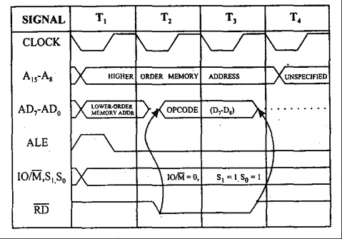
Opcode Fetch (OF) machine cycle of 8085:
Each instruction of the microprocessor has one byte Opcode. The Opcode is stored in memory. In order to fetch the Opcode from memory, processor executes the Opcode Fetch machine cycle. So, every instruction starts with Opcode Fetch machine (OFM) cycle. The time taken by the microprocessor to execute the Opcode Fetch cycle is 4T (T- states). Inorder to fetch the Opcode from memory, the first 3 T-states are used. The remaining T-state is used for internal operations by the microprocessor.
The timing diagram for Opcode Fetch machine cycle is shown in figure.
The steps in Opcode Fetch machine cycle are given in table.
S. No | T state | Operation |
1 | T1 | The microprocessor places the higher order 8-bits of the memory address on A15 – A8 address bus and the lower order 8-bits of the memory address on AD7 – AD0 address / data bus. |
2 | The microprocessor makes the ALE signal HIGH and at the middle of T1 state, ALE signal goes LOW. | |
3 | The status signals are changed as IO/𝑀’ = 0, S1 =1 and S0 = 1. These status signals do not change throughout the OF machine cycle. | |
4 | T2 | The microprocessor makes the RD’ line LOW to enable memory read and increments the Program Counter. |
5 | The contents on D7 – D0 (i.e. the Opcode) are placed on the address / data bus. | |
6 | T3 | The microprocessor transfers the Opcode on the address / data bus to Instruction Register (IR). |
7 | The microprocessor makes the RD’ line HIGH to disable memory read. | |
8 | T4 | The microprocessor decodes the instruction. |
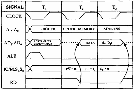
Memory Read Machine Cycle of 8085:
Single byte instructions require only Opcode Fetch machine cycles. But, 2-byte and 3-byte instructions require additional machine cycles to read the operands from memory. The additional machine cycle is called Memory Read machine cycle. For example, the instruction MVI A, 50H requires one OF machine cycle to fetch the operand from memory and one MR machine cycle to read the operand (50H) from memory. The MR machine cycle takes 3 T-states.
The timing diagram for Memory Read machine cycle is shown in figure.
Timing Diagram for Memory Read Machine Cycle
The steps in Memory Read machine cycle are given in table.
S. No | T state | Operation |
1 | T1 | The microprocessor places the higher order 8-bits of the memory address on A15 – A8 address bus and the lower order 8-bits of the memory address on AD7 – AD0 address / data bus. |
2 | The microprocessor makes the ALE signal HIGH and at the middle of T1 state, ALE signal goes LOW. | |
3 | The status signals are changed as IO/𝑀’ = 0, S1 =1 and S0 = 0. These status signals do not change throughout the memory read machine cycle. | |
4 | T2 | The microprocessor makes the RD’ line LOW to enable memory read and increments the Program Counter. |
5 | The contents on D7 – D0 (i.e. the data) are placed on the address / data bus. | |
6 | T3 | The data loaded on the address / data bus is moved to the microprocessor. |
7 | The microprocessor makes the RD’ line HIGH to disable the memory read operation. |
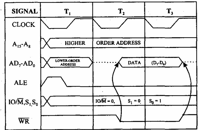
Memory Write Machine Cycle of 8085:
Microprocessor uses the Memory Write machine cycle for sending the data in one of the registers to memory. For example, the instruction STA 5000H writes the data in accumulator to the memory location 5000H. The MW machine cycle takes 3 T-states.
The timing diagram for Memory Write machine cycle is shown in figure.
Timing Diagram for Memory Write Machine Cycle
The steps to disable the memory write machine cycle are given in table.
S. No | T state | Operation |
1 | T1 | The microprocessor places the higher order 8-bits of the memory address on A15 – A8 address bus and the lower order 8-bits of the memory address on AD7 – AD0 address / data bus. |
2 | The microprocessor makes the ALE signal HIGH and at the middle of T1 state, ALE signal goes LOW. | |
3 | The status signals are changed as IO/𝑀’ = 0, S1 =0 and S0 = 1. These status signals do not change throughout the memory write machine cycle. | |
4 | T2 | The microprocessor makes the 𝑊𝑅’ line LOW to enable memory write. |
5 | The contents of the specified register are placed on the address / data bus. | |
6 | T3 | The data placed on the address / data bus is transferred to the specified memory location. |
7 | The microprocessor makes the 𝑊𝑅’ line HIGH to disable the memory write operation. |
I/O Read Machine Cycle of 8085
Microprocessor uses the I/O Read machine cycle for receiving a data byte from the I/O port or from the peripheral in I/O mapped I/O systems. The IN instruction uses this machine cycle during execution. The IOR machine cycle takes 3 T-states.
The timing diagram for I/O Read machine cycle is shown in figure.
Timing Diagram for I/O Read Machine Cycle
The steps in I/O Read machine cycle are given in table.
S. No | T state | Operation |
1 | T1 | The microprocessor places the address of the I/O port specified in the instruction on A15 – A8 address bus and also on AD7 – AD0 address / data bus. |
2 | The microprocessor makes the ALE signal HIGH and at the middle of T1 state, ALE signal goes LOW. | |
3 | The status signals are changed as IO/𝑀’ = 0, S1 =1 and S0 = 0. These status signals do not change throughout the I/O read machine cycle. | |
4 | T2 | The microprocessor makes the 𝑅𝐷’ line LOW to enable I/O read. |
5 | The contents on D7 – D0 (i.e. the data) are placed on the address / data bus. | |
6 | T3 | The data loaded on the address / data bus is moved to the microprocessor ie., to the accumulator. |
7 | The microprocessor makes the 𝑅𝐷’ line HIGH to disable the I/O read operation. |
I/O Write Machine Cycle of 8085
Microprocessor uses the I/O Write machine cycle for sending a data byte to the I/O port or to the peripheral in I/O mapped I/O systems. The OUT instruction uses this machine cycle during execution. The IOR machine cycle takes 3 T-states. The timing diagram for I/O Write machine cycle is shown in figure.
Timing Diagram for I/O Write Machine Cycle
The steps in I/O Read machine cycle are given in table.
S. No | T state | Operation |
1 | T1 | The microprocessor places the address of the I/O port specified in the instruction on A15 – A8 address bus and also on AD7 – AD0 address / data bus. |
2 | The microprocessor makes the ALE signal HIGH and at the middle of T1 state, ALE signal goes LOW. | |
3 | The status signals are changed as IO/𝑀’ = 0, S1 =0 and S0 = 1. These status signals do not change throughout the I/O write machine cycle. | |
4 | T2 | The microprocessor makes the 𝑊𝑅’ line LOW to enable I/O write. |
5 | The contents of the Accumulator are placed on the address / data bus. | |
6 | T3 | The data placed on the address / data bus is transferred to the specified I/O port. |
7 | The microprocessor makes the 𝑊𝑅’ line HIGH to disable the I/O write operation |
Tags:
Microprocessors