
Operating Principles of I2L gates
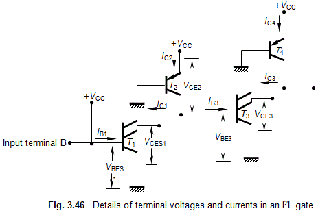 Now, let the input voltage Vi = 0 V. This makes transistor T1 to be in OFF-state, and IC2 to flow through the base of T2. Thus, VBE3 = VBES3 = 0.8 V. This makes VCE1 = VBES3 = logic 1, and VCE3 = VCES3 = logic 0. Thus, the transistors perform inversion operation, with logic 0 = VCES = 0.2 V, and logic 1 = VBES = 0.8 V. The voltage swing of this gate, therefore, is
Vswing=VBES – VCES = 0.8 – 0.2 = 0.6 volt

I2L Gates for Performing Multiple Functions

Integrated Injection Logic Operation is explained as follows. To understand the working of a typical I2L gate, consider Fig. 3.46, which consists of five transistors, connected as shown. It can be seen that the base current IB1 of T1 is derived from +VCC through the input terminal B. The base-bias current IB3 of transistor T3 and the collector current IC1 of T1 are obtained from the collector current of transistor T2 whose injector (emitter) also is connected to +VCC.
If IB1 is sufficient, the base-to-emitter voltage VBE1 of T1 will become the saturation base-emitter voltage VBES1 (= 0.8 volt), and in this condition, its collector-to-emitter voltage VCE1 will become saturation base-emitter voltage VCES1 (= 0.2 volt). So, we find that T1 is in the ON-state and its output is at logic-0 level. Since VCES1 = 0.2 volt, the collector current IC2 of T2 will flow through the collector of T1 as IC1, and VBE3 of T3 = 0.2 V = VCES1. This means that at this moment, T3 is OFF and its collector-emitter voltage VCE3 = 0.8 volt.
Vswing=VBES – VCES = 0.8 – 0.2 = 0.6 volt
It can be seen that the logic swing of I2L gates is very low and this is a major defect of these gates.
I2L Gates for Performing Single Function
Figure 3.47 shows a typical I2L gate which performs the single function of logical inversion (or NOTing). In this case, MOS transistor N1 performs the inversion of input A to produce the output A'. MOS transistor N2 performs inversion of this output and produces A again. Thus the circuit shown in Fig. 3.47 performs the operation of double inversion.
I2L Gates for Performing Multiple Functions
Figure 3.48 shows a multi-function I2L gate that can perform the operations of NOT, AND, NAND, and NOR. Notice that only transistors are used. However, an external resistor R may be used to derive the currents required for all the PNP transistors from a single +VCC supply. Notice that the PNP transistors are not shown in Fig. 3.48.
Transistors T1 and T2 invert inputs A and B to produce A' and B′, respectively. One collector of T1 and one collector of T2 are now tied together to perform ANDing to produce the NAND output of A'B′. Using De Morgan, we find that this operation is also equivalent to the NOR output (A+B)′.. The other collectors are used to drive respectively, transistors T3 and T4, which now invert A' and B′ to give the AND output AB. T5 inverts AB to give (AB)′. We notice that all logical functions can be obtained from a single I2L chip. Since only transistors are used the packing density of I2L gate is seen to be comparable to that of the MOS logic; but the voltage swing is only 0.8 − 0.2 = 0.6 volt. Due to this small swing in the output voltage, the I2L technology has not progressed very much, and is not in much use now.
Advantages of I2L Gates
· Since I2L gates are made up only of BJTs, they possess high speed of operation.
· Because only transistors are used for the construction, I2L gates have high packing density, and are hence suitable for construction of VLSI circuits.
· Very low power-supply requirement (1 volt) .
· Low power dissipation.
· Number of processing steps required is small; hence cost per gate is low.
· Several functions are possible on the same chip.
· Using bipolar technology, it is possible to combine I2L gates with other logic families.
Disadvantages of I2L Gates
· Very low voltage swing (≈ 0.6 V); the swing is between VBES (0.8 V) and VCES (0.2 V).
· Lower packing density than NMOS.
· Lower noise margin.
· External resistance required for proper functioning.
· I2L technology, at present, is dormant.