
In Sections 3.1 to 3.17, we have discussed logic families that belong to the category of saturating logic. The active devices (BJTs and FETs) used in the logic gates belonging to this category operate in their saturation and cut-off modes. To turn-on and turn-off these devices require more time than devices that operate in their active region of operation. So gates that operate in the saturating mode are relatively slow. This suggests that devices that operate in their active region of operation are much faster than saturating-mode devices. Emitter-coupled logic (ECL) family is a logic family that makes use of differential amplifiers operating in their active mode for the construction of logic gates.
 Consider Fig. 3.50, which shows the details of the circuit connections and node voltages required for the analysis. Let the input A be at logic-0 level. This makes T2 OFF and T3 ON. Let us assume that transistor T3 is operating in its active region. We also assume that its base-emitter voltage VBE3 = 0.7 V. Then from Fig. 3.50, we find that voltage at node X,
VX = – VR – VBE3 = –1.15 – 0.7= –1.85 volt

VZ = 0.7 V
Vout-swing = – 0.7 – (–1.5) = 0.85 V
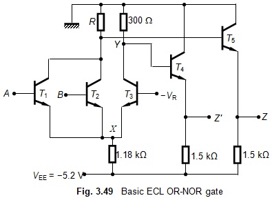
Figure 3.49 shows the circuit diagram of an OR-NOR gate using ECL. This is the basic gate in the ECL family. As stated above, the ECL OR-NOR gate consists basically of two differential amplifiers that drive two emitter followers. From Fig. 3.49, we find that bipolar junction transistors T1 and T3 form the first differential amplifier and T2 and T3 form the second. These differential amplifiers drive two emitter-follower stages comprising of transistors T4 and T5 to deliver complementary outputs Z' and Z. The load resistance of T3 is 300 ohms. For the ideal OPAMP, the load of T2 must also be of 300 ohms. However, in practice, it will be less than this, as will be shown later.
One of the main features of the ECL gate is that the collector terminals of its transistors are grounded, and a DC voltage of –5.2 V is applied to the emitters. This negative supply voltage makes the calculations slightly difficult, since mostly we are familiar with positive supply voltages. However, a systematic approach in this case will give the required results.
It may be noticed that ECL gates are used to produce multiples output functions (such as OR-NOR) from a single gate. Since two or more transistors are fabricated on a single semiconductor region, I2L is also called as merged-transistor logic (MTL).
Working Principles of the ECL OR-NOR Gate
The ECL gate, as stated above, is basically a differential amplifier, working in its active region. Since it is operating in its active region, the voltage swing of an ECL gate is as low as ±200 mV. Also, it dissipates quite a large amount of power as the circuit draws heavy collector current during the entire period of its operation. There is no OFF-state for the ECL gates to reduce power loss.
The main advantage of the ECL gate is that it was the fastest logic circuit prior to the advancement of CMOS chips. Typical speed of ECL gates lie in the range of few GHz. However, currently CMOS chips are available with much higher speed than that of the ECL chips. The very low power and supply-voltage requirements have made CMOS logic more popular now.
VX = – VR – VBE3 = –1.15 – 0.7= –1.85 volt
The supply voltage of ECL gate is fixed at –5.2 V. Therefore, the voltage drop across the 1.18-kΩ emitter resistor of the differential pair is
V1.18 kΩ = –VX – (–VEE) = – 1.8 – (–5.2) = 3.35 V
Hence current I through the 1.18-kΩ resistor is given by
I = 3.35 V/1.18 kΩ = 2.84 mA
This 2.84 mA flowing through the collector of T3 will produce a drop of 0.85 V across its 300-ohm collector resistor. Thus, the node Y is at –0.85 V with respect to ground under this condition. Assuming T4 to be ON this time, the voltage output at node Z (emitter of T4) is:
VZ = –0.85 –0.7 = –1.5 V
This is the logic-0 level of the ECL gate. Notice that in the logic-0 level, all the transistors operate in their active region rather than in cut-off and saturation.
That the transistor T2 (or T1) is indeed in logic 0 may now be computed by considering the fact that with VA, the voltage at point A = −1.5 V and VX = –1.85 V,
VBE1 = VBE2 = –1.5 – (1.85) = 0.3 V
where VBE1 and VBE2 are the base-emitter voltages of T1 and T2, respectively. It can be seen that the minimum base-emitter voltage of a transistor to start conducting is 0.4 to 0.5 V and therefore, with VBE = 0.3 V, both T1 and T2 are indeed in the OFF state.
Now, let us consider the situation when A = 1. This makes T1 ON, and the collector current switches from the 300-ohms resistor to resistor R. With T3 OFF, its collector voltage VY is at ground potential, as no current is now flowing through the 300-ohms resistor. Again, with T4 in the active region, VBE4 = 0.7 V. Since T4 is an emitter-follower, the output voltage VZ = VBE4 = 0.7 V. Thus, the output voltage for logic 1 at A is given by:
VZ = 0.7 V
We now conclude that for the ECL OR/NOR gate, the logic levels are given by:
Logic-0 level = – 1.5 V
Logic-1 level = – 0.7 V
The above figures illustrate that the output swing of an ECL gate is only
Vout-swing = – 0.7 – (–1.5) = 0.85 V