
The NMOS OR Gate Circuit
Figure 3.23(a) shows a two-input OR gate using NMOS FETs and 3.23(b) shows its equivalent using switches. It may be noticed in this case also that NMOS transistors are used to replace the mechanical switches and the load resistor. We find that, if A = 0 and B = 0 (i.e., A and B have 0-volt inputs), transistors T1and T2 will remain OFF. Then, output Z = 0 volt (logic 0). However, when A = 0 and B = 1, or B = 0 and A = 1, or A = B = 1, either one or both of transistors T1 and T2 conduct and develop +VDD, across the load transistor T3. This means that the output Z = logic 1. This may be summarized as given in Table 3.4. The logic relations given in Table 3.4 are seen to be that of the OR operation. So, we conclude that the logic gate shown in Fig. 3.23(a) performs the positive-logic OR function.
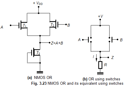 Table 3.4 NMOS OR
Figure 3.23(a) shows a two-input OR gate using NMOS FETs and 3.23(b) shows its equivalent using switches. It may be noticed in this case also that NMOS transistors are used to replace the mechanical switches and the load resistor. We find that, if A = 0 and B = 0 (i.e., A and B have 0-volt inputs), transistors T1and T2 will remain OFF. Then, output Z = 0 volt (logic 0). However, when A = 0 and B = 1, or B = 0 and A = 1, or A = B = 1, either one or both of transistors T1 and T2 conduct and develop +VDD, across the load transistor T3. This means that the output Z = logic 1. This may be summarized as given in Table 3.4. The logic relations given in Table 3.4 are seen to be that of the OR operation. So, we conclude that the logic gate shown in Fig. 3.23(a) performs the positive-logic OR function.
A | B | Z |
0 0 1 1 | 0 1 0 1 | 0 1 1 1 |
T3 NMOS gate is connected to gnd (logic 0), then how can it be ON? since NMOS requires logic 1 at gate Voltage to make Vgs>0
ReplyDelete