
The NMOS NOR Gate Circuit:
Figure 3.24(a) shows a two-input NOR gate using NMOS FETs replacing the mechanical switches of the two-input NOR gate shown in Fig. 3.24(b).
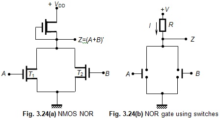
As in the previous cases, switching transistors T1 and T2 are of the enhancement type and T3, which acts as the load resistance, is of the depletion type. If A = 0 and B = 0 (i.e., both A and B have 0-volt inputs), transistors T1 and T2 will remain OFF. Then, the output across the load Z = +VDD (logic 1). However, when A = 0 and B = 1, B = 0 and A = 1, or A = B = 1, either T1 or T2 or both T1 and T2 will conduct as the case may be and the output Z = 0 volt (logic 0). These conditions are summarized as given in Table 3.5. The logic relations given in Table 3.5 that the logic gate shown in Fig. 3.24(a) performs the positive-logic NOR operation.
A | B | Z |
0 0 1 1 | 0 1 0 1 | 1 0 0 0 |