
AND FUNCTION:
After having defined the positive and negative logic schemes, let us now define the basic logic operations. We begin our explanation with the AND operation, which is defined by the logical expression:
Z = A∙B = AB (2)
Equation (2) can be read as Z equals A AND B. The dot (×) sign in the equation represents a Boolean product or AND operation. Even though we may read this also as A into B to indicate a multiplication operation, strictly speaking, it is a wrong usage in binary. Now, consider the relations:
0 ∙ 0 = 0
0 + 0 = 0
A resistive load R and a DC power supply +V are connected in series with this parallel combination. Current I flows through R and develops a voltage drop of +V volts across it when either A or B or both are closed. These three conditions may be expressed in the form: Z = 1, when A = 0, B = 1, or A = 1, B = 0, or A = B = 1. If both the switches are open, then no current will flow through the load, and hence the output voltage Z = 0 volt = logic 0. This represents a positive-logic OR operation. Figure shows the logic symbol of the two-input OR gate.

THE NOT (INVERSION) OPERATION


After having defined the positive and negative logic schemes, let us now define the basic logic operations. We begin our explanation with the AND operation, which is defined by the logical expression:
Z = A∙B = AB (2)
Equation (2) can be read as Z equals A AND B. The dot (×) sign in the equation represents a Boolean product or AND operation. Even though we may read this also as A into B to indicate a multiplication operation, strictly speaking, it is a wrong usage in binary. Now, consider the relations:
0 ∙ 1 = 0
1 ∙ 0 = 0
1 ∙ 1 = 1 (3)
These are valid Boolean relations and represent the binary product of bits (binary digits) 0 and 1.
Generally, various English alphabets are used to represent binary 1s and the same alphabets, added with some special identification marks, are used to represent binary 0s. For example, if 1 is represented by letters a, b, x, y, etc., then 0 may be represented by characters a¢, b¢, etc. Bit 0 is usually called as the complement of bit 1, and vice versa. In this text, we will be mainly using symbols of the form a¢, y¢, etc. to represent complementary variables.
Generally, various English alphabets are used to represent binary 1s and the same alphabets, added with some special identification marks, are used to represent binary 0s. For example, if 1 is represented by letters a, b, x, y, etc., then 0 may be represented by characters a¢, b¢, etc. Bit 0 is usually called as the complement of bit 1, and vice versa. In this text, we will be mainly using symbols of the form a¢, y¢, etc. to represent complementary variables.
The truth table related to the AND function is shown in Table Using the entries in this table, we test the validity of the AND expression given by Eq. (2). It can be seen that the entries in Table are the same as those given in Eq. (3).
Table Truth table of AND function
A | B | Z = AB |
0 | 0 | 0 |
0 | 1 | 0 |
1 | 0 | 0 |
1 | 1 | 1 |
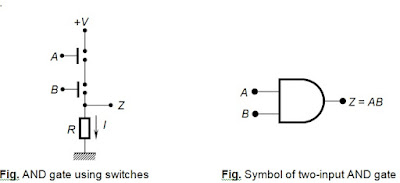
Using the circuit shown in Fig., we now prove the relations given in Table. In Fig., we find that switches A and B and a resistor R are connected in series with a DC power supply of +V volts. Assuming positive-logic operation, let 0 represent an open or OFF switch and 1 represent a closed or ON switch.

Now, consider the situation in which both the switches are open. This condition may be expressed as A = B = 0. In this condition, current I will not flow through R and hence the output voltage Z = 0 volt ≡ logic 0 (the symbol “ ≡ ” stands for equivalent to). It can be seen that I = 0, (and hence Z = 0) even when one of the switches is closed and the other remains open. There are two conditions in this case, and these two conditions may be expressed by the logic expressions A = 0, B = 1, and A = 1, B = 0, respectively. Current I will flow through R only when both the switches are closed; and then the output voltage Z = IR = +V. This condition may be expressed by the logic expression Z = 1, when A = B = 1,
Combining all the conditions given above, we find that the switching circuit shown in Fig. performs the logic AND operation. Figure shows the logic symbol of the two-input AND gate.
THE OR FUNCTION
Let us now consider the logic OR operation, which is defined by the expression:
Z = A + B (4)
Equation (4) can be read as Z equals A OR B. The plus (+) sign in the equation represents a Boolean summing (i.e., OR) operation. Even though we may read this also as A plus B to indicate a summing operation, strictly speaking, it is a wrong usage in binary. Now, consider the relations
0 + 1 = 0
1 + 0 = 0
1 + 1 = 1 (5)
It can be seen that the relations given above are valid summing relations in the binary number system. Hence we may say that the statement Z = A OR B may also be stated as Z = A plus B. The truth table of the OR function is shown in Table. It can be seen that the entries of Table are the same as those given in Eq. (5). Figure shows an OR gate using two switches A and B connected in parallel to each other.
Table Truth table of OR function
A | B | Z = A + B |
0 | 0 | 0 |
0 | 1 | 1 |
1 | 0 | 1 |
1 | 1 | 1 |
A resistive load R and a DC power supply +V are connected in series with this parallel combination. Current I flows through R and develops a voltage drop of +V volts across it when either A or B or both are closed. These three conditions may be expressed in the form: Z = 1, when A = 0, B = 1, or A = 1, B = 0, or A = B = 1. If both the switches are open, then no current will flow through the load, and hence the output voltage Z = 0 volt = logic 0. This represents a positive-logic OR operation. Figure shows the logic symbol of the two-input OR gate.

THE NOT (INVERSION) OPERATION
The NOT (negation) operation is characterized by an inverting operation. If a given function A represents a closed switch, then NOT of A represents an open switch and vice versa. The function NOT of A may be represented symbolically. Figure shows a mechanical switch connected in series to a resistor R and a DC supply voltage of +V volts. Whenever switch A is open (i.e., A ≡ 0), no current (I) flows through R. Then, output Z = +V (≡ 1). Thus when input A = 0, we find that output = 1 = A′. Now, if A is closed ( ≡ 1), t I will flow through R and switch A. Since A is closed, it will act as a dead short across the output terminals making Z = 0 volt ≡ 0 = A′. Thus we find that the circuit shown in Fig. performs the NOT operation.
Figure shows an implementation of the positive-logic NOT gate using an NPN transistor switch. When the input of the transistor is 0 V (i.e., A = 0), its output Z = +VCC volts (≡ 1 = A′). When A = +VCC volts (≡ 1 = A′), its output is 0 volt (representing 0 = A′)

The truth table of the NOT gate is shown in Table and its logic symbol is shown in Fig. The bubble (small circle) at the tip of the triangle represents a negation (inverting) operation.
Table Truth Table of NOT gate
A | A′ |
1 0 | 0 1 |
THE NAND (NOT AND) FUNCTION
Consider the AND truth table shown in Table. Let the entries in the third column of this table (representing output Z) be inverted (i.e., 1s changed to 0s and 0s changed to 1s). The resultant new truth table is shown in Table
Table Truth table of NAND function
A | B | Z = (A B)′ |
0 | 0 | 1 |
0 | 1 | 1 |
1 | 0 | 1 |
1 | 1 | 0 |
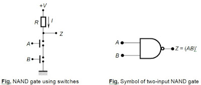
This table describes the operation of a NAND gate. NAND operation is obtained by combining an AND gate in series with a NOT gate. It can be seen that the NOT gate inverts the outputs of the AND gate to yield the NAND (NOT of AND) function. The NAND function is generally denoted as (AB)′, where the apostrophe symbol (′) denotes a negation, inversion, or complementing operation.
Figure shows a NAND gate constructed using mechanical switches. It can be seen that this circuit is a modification of the AND circuit shown in Fig. In the AND gate, resistor R is connected below the switches. Since NAND is an inversion of AND, the position of R is inverted, i.e., it is moved to the position above the switches. Logic symbol of the NAND is shown in Fig.

THE NOR (NOT OR) FUNCTION
The working of the circuit shown in Fig. can be described as follows. Let initially, A and B be open. This means A = B = 0. In this condition, no current will flow through the circuit and hence I = 0. This makes output Z = +V ≡ logic 1. The same condition, viz., I = 0 and Z = +V ≡ logic 1, prevails even when A = 1 and B = 0, or A = 0 and B = 1. However, when A = B = 1, both the switches are closed and I flows through the circuit. It can be seen that in this condition, the output is shorted by the closed switches; hence Z = 0 volt ≡ logic 0. These actions represent a NAND operation. It may be observed that a NOT gate can be obtained by shorting all the input terminals of a NAND gate.
Figure shows a NOR gate constructed using mechanical switches. It can be seen that this circuit is a modification of the OR circuit shown in Fig. In the OR gate, resistor R is connected below the switches. Since NOR is an inversion of OR, the position of R is inverted, i.e., it is moved to the position above the switches. Logic symbol of the NOR is shown in Fig.The working of the circuit shown in Fig. can be described as follows. Let initially, A and B be open. This means A = B = 0. In this condition, no current will flow through the circuit and hence I = 0. This makes output Z = +V ≡ logic 1. The same condition, viz., I = 0 and Z = +V ≡ logic 1, prevails even when A = 1 and B = 0, or A = 0 and B = 1. However, when A = B = 1, both the switches are closed and I flows through the circuit. It can be seen that in this condition, the output is shorted by the closed switches; hence Z = 0 volt ≡ logic 0. These actions represent a NAND operation. It may be observed that a NOT gate can be obtained by shorting all the input terminals of a NAND gate.
Consider the OR truth table shown in Table. Let the entries in the third column of this table (representing output Z) be inverted (i.e., 1s changed to 0s and 0s changed to 1s), as shown. Table shows the truth table incorporating these changes. This table describes the operation of a NOR gate. NOR operation is obtained by combining an OR gate in series with a NOT gate. It can be seen that the NOT gate inverts the outputs of the OR gate to yield the NOR (NOT of OR) function. The NOR function is generally denoted as (A + B)′, where the apostrophe (′) denotes a negation, inversion or complementing operation.
Truth Table of NOR function
A | B | Z = (A + B)′ |
0 | 0 | 1 |
0 | 1 | 0 |
1 | 0 | 0 |
1 | 1 | 0 |

The working of the circuit shown in Fig. can be described as follows. Let initially, A and B be open. This means A = B = 0. In this condition, no current will flow through the circuit and hence I = 0, and Z = +V ≡ logic 1. However, when A = 1 and B = 0, A = 0 and B = 1, or A = B = 1, I will flow through the circuit and Z = 0 volt ≡ logic 0, It can be seen that under these conditions, the output is shorted by the closed switch (or switches); hence Z = 0 volt ≡ logic 0. These actions represent a NOR operation. It may be noticed that a NOT gate can be obtained by shorting the input terminals of a NOR gate.
UNIVERSAL GATES:
It can be seen that two NAND gates connected in series will give us an AND gate. However, two AND gates connected in series can not produce a NAND gate. Similarly, two NOR gates connected in series will give us an OR gate. But, two OR gates connected in series can not produce a NOR gate.
It may be noted in this context that a NOR operation can be converted to a NAND operation and vice versa. For such NAND-NOR conversions, we make use of a set of fundamental Boolean laws known as the De-Morgan’s laws.
It can now be seen that complex logic expressions can be realized by interconnecting connecting NAND (or NOR) gates alone in series, in parallel, and in combined forms. Therefore, NAND gates and NOR gates are called as universal gates.