
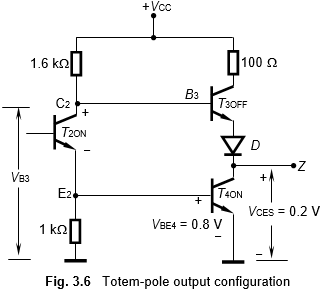
Reason for Using the Totem-Pole Output Configuration:
 Now consider the situation when the input is 0 and the output of the NAND gate is 1. This transition from 0 volt to +VCC volts will be completed only after CL has been charged fully to +VCC through RL. If RL is a pure resistor, CL will take a long time to charge fully because usually RL will be large to reduce large power dissipation in ICs. This technique of using a passive component RL for charging CL is called passive pull-up.
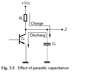
Consider Fig. 3.5, which shows T3 (one of the totem-pole output transistors) being replaced with a load resistor RL. Now, assume that the input terminals A and B are together and a trigger pulse applied to it. In an ideal situation when a trigger is applied, we expect the NAND gate to switch suddenly from the OFF-state to the ON-state, and vice versa. However, in a practical situation, this is not the case. We know that a capacitance exists in between two wires carrying currents of opposite nature and separated by a dielectric such as air. Using this concept, we find that several parasitic capacitances exist across the output section of the TTL gate. The total effect of these capacitances is represented by the single load capacitance CL shown in Fig. 3.5.
Now, when a trigger pulse is applied to the input of the TTL gate to produce transition of the state, we find that CL must be charged or discharged first before the transition is completed. First, let us consider a positive trigger pulse being applied to the input of the gate. As we have discussed earlier, this turns T4 ON, and CL discharges through transistor T4. We know that the ON-resistance of a BJT is very small and hence the discharge-time is also very small. Therefore, CL discharges at a fast rate through T4.
In the standard TTL NAND gate, RL is replaced with transistor T3. Since an active device is used for charging CL, this operation is called as active-pull-up. Thus active-pull-up consists of T3 on top of T4. When a 0-input is applied, the output rises from 0 to +VCC through T3, which is now in the ON-state. As explained above, T3 has a low ON-resistance and hence charges CL fast. Thus, the active-pull-up produces faster transition in the switching between states. This makes TTL gates the fastest saturation-logic family.
Consider T2 to be ON. Then, heavy collector current flows through T2 to develop enough potential at emitter E2 which turns T4 ON. Since T4ON requires its base-emitter voltage VBE4 = VBES, where VBES is the saturation base-emitter voltage (= 0.8 V), we find that E2 is clamped at 0.8 V. Therefore, VC2 (voltage at C2) = VB3 (voltage at the base of T3 with respect to ground) is given by
Need for the 100-ohm Resistor on Top of T3
If there were only transistors in the output stage, while switching from ON-to-OFF, or OFF-to-ON states, there will be moments when the output transistors become dead short across the supply before steady state is achieved. This situation drives heavy current through transistors T3 and T4 and destroys them. To prevent this, we use the 100-ohm resistor, which limits the output current to a safe value.
Use of Diode D
Consider the situation when there is no diode, and T4 is ON. At this time, we want T3 to be OFF. To investigate this, we consider Fig. 3.6, which shows the output section of the TTL NAND gate.
Consider T2 to be ON. Then, heavy collector current flows through T2 to develop enough potential at emitter E2 which turns T4 ON. Since T4ON requires its base-emitter voltage VBE4 = VBES, where VBES is the saturation base-emitter voltage (= 0.8 V), we find that E2 is clamped at 0.8 V. Therefore, VC2 (voltage at C2) = VB3 (voltage at the base of T3 with respect to ground) is given by
VC2 = VBES of T4 + VCES of T2 = 0.8 V + 0.2 V = 1.0 V
Now, the collector of T4 (and hence the emitter of T3) is at VCES (= 0.2 V) with respect to ground. Therefore, VBE3 (base-emitter voltage of T3) = 1.0 – 0.2 = 0.8 V. A voltage of 0.8 V between the base and emitter of T3 means that it is in saturation. However, our assumption was that T3 was in the OFF-state. Hence, to ensure that T3 is indeed in the OFF-state, diode D is introduced in between the emitter of T3 and the collector of T4. The drop across the diode is usually 0.6 V so that T3 is indeed in the OFF-state with its base having not enough voltage to turn it ON.