Low-Power Dissipation in CMOS Logic Gates
CMOS logic gates are currently the most popular forms of logic gates because of their advantages over other logic families. One of the main features of CMOS gates is its low-power dissipation capability. This feature is explained below.
CMOS gates are constructed, as explained above, with NMOS upon PMOS or vice versa. For example, consider the CMOS inverter shown in Fig. 3.26. This is redrawn here as shown in Fig. 3.30(a) for illustration. Figure 3.30(b) shows an approximate equivalent inverter network using mechanical switches. In this, we have represented the PMOS transistor using a closed switch and the NMOS transistor using an open switch. We also find that the two switches are ganged together by a push/pull lever, which can be operated to open the PMOS switch and close the NMOS switch or vice versa. Assuming push ≡ logic 0 and pull ≡ logic 1, we find that the circuit shown in Fig. 3.30(b) performs inversion.
It can be seen from Fig. 3.30(b) that only one of the switches remains closed and the other remains open at any instant under consideration,. This means that, no current will flow through the circuit at any instant of time, and hence no power loss will occur in the circuit. However this is too ambitious a statement to be realized in practice
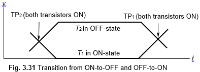
In actual practice, a very small amount of leakage current will flow through the device, especially when the transistors are turned-on or turned-off. For example, let initially the PMOS be ON and the NMOS be OFF. We assume that the drain current ID = 0. Now, let a trigger applied to the gate of NMOS turns it ON suddenly. At this time, the PMOS, which was conducting previously, still continues to conduct for a little more time before it turns OFF. So, we find that both the transistors are conducting simultaneously for a very small interval of time. During this period some power will be drained from the battery and dissipated in the transistors. But this is usually negligibly small.
Figure 3.31 shows two situations when both the transistors remain in the ON-state simultaneously; this occurs at transitions points TP1 and TP2, as shown. TP1 is the instant at which T1 jumps up from its ON-state to OFF-state and T2 jumps down from its OFF-state to ON-state. Similarly, TP2 is the instant at which T2 jumps up from its ON-state to OFF-state and T1 jumps down from its OFF-state to ON-state.
From data manuals of CMOS gates, it is found that the drain current of CMOS transistors is in the range of nA to pA (10−9 to 10−12). Power dissipation of COMOS gates is about a few pW. With the advent of modern technology, packing density of CMOS gates has been found to be extremely high and the speed of operation has reached the GHz range.


